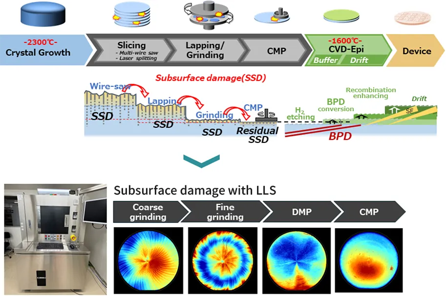
Subsurface damage Measurement with laser Light Scattering (LLS)method
From ingot slicing through subsequent wafer processing steps, processing-induced damaged layers are generated on the wafer surface. It has been reported that these damaged layers can act as the origin of killer defects during the Epi-CVD process. We have independently developed laser Light Scattering –based visualization system for processing-induced strain generated during wafer processing. By using this system, processing-induced strain over the entire wafer surface can be visualized non-destructively.
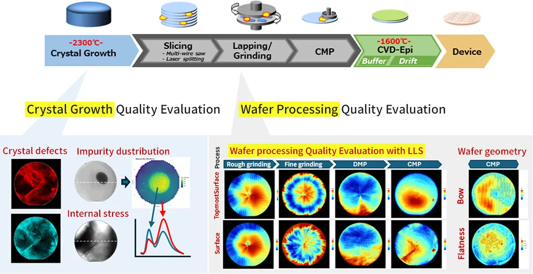
Comprehensive Diagnosis from Two Perspectives
—Crystal and Processing— LLS metod with Other Measurement Techniques.